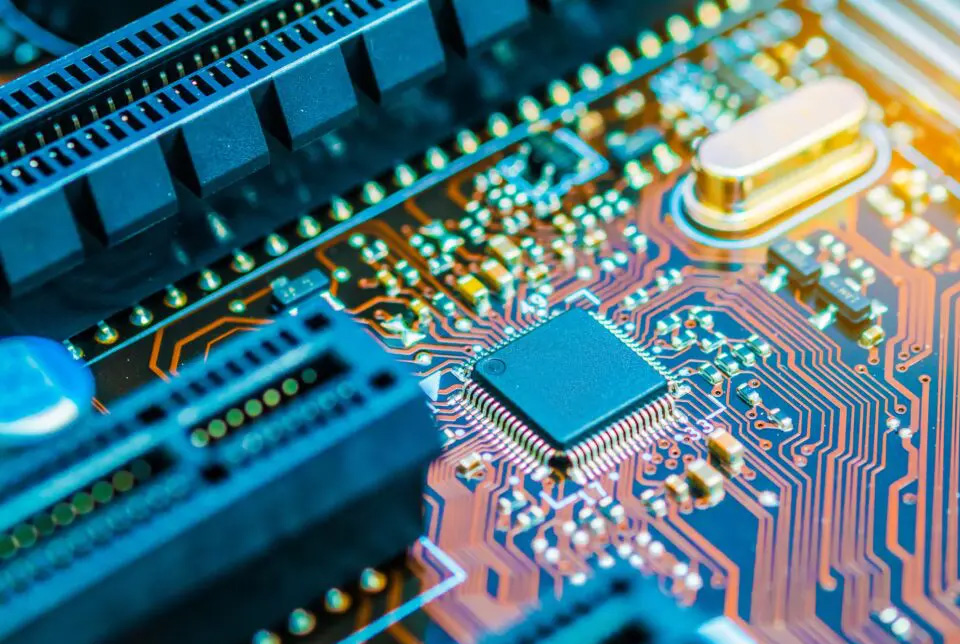
Electronic & Semiconductor Cleaning
Water- & solvent based cleaning solutions dedicated for the electronic assembly & semiconductor industry and suited for your desired process.
Electronic & Semiconductor Cleaning Solutions for Every Manufacturing Challenge
Effective cleaning in electronics and semiconductor manufacturing is essential for removing contaminants that could impact performance, reliability, longevity, and overall device functionality, directly influencing production efficiency and component integrity.
Select subsegment :
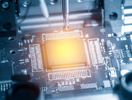
PCB Defluxing & Cleaning
Defluxing is crucial in cleaning solutions for effectively removing residual flux and contaminants from sensitive semiconductor components, with INVENTEC offering advanced technologies that ensure optimal performance, enhanced reliability, and longevity of electronic devices, even in the most demanding applications.
Discover how advanced PCB defluxing and flux cleaning solutions enhance the reliability, performance, and longevity of your electronic assemblies in today’s complex manufacturing environment…
Learn more
Related products & services
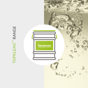
TOPKLEAN EL 20P
- Removal of flux residues
- Co-solvent process
- Very high cleaning power & sustainable solution
![]()
PROMOCLEAN DISPER 707

TOPKLEAN EL 20D
PROMOCLEAN DISPER 800
PROMOCLEAN TP 61
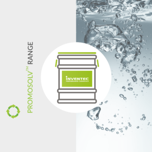
PROMOSOLV 70ES
- Removal of flux residues
- Vapor phase process
- Balanced performance
- 3M Novec 71DA, Novec 72DA replacement

TOPKLEAN EL 10F

PROMOSOLV DE4

Power Electronics Cleaning
Cleaning power electronics is vital to ensure optimal performance and longevity by preventing the buildup of dust, dirt, and other contaminants that can interfere with heat dissipation and electrical connections; INVENTEC offers specialized solutions to support this critical maintenance process.
Discover how effective power electronics cleaning enhances the reliability, efficiency, and lifespan of power electronic systems using advanced solutions like DCB cleaning and semiconductor cleaning…
Learn more
Package Cleaning
Package cleaning in semiconductor cleaning solutions plays a key role in removing contaminants from BGAs, CMOS, and flip chips—factors that can affect device performance, yield, and reliability during the final stages of production; INVENTEC provides advanced solutions specifically designed to meet these critical cleaning needs.
Effective cleaning package solutions are essential in semiconductor manufacturing to ensure the reliability, performance, and longevity of devices built with advanced package technology…
Learn more
Maintenance Cleaning
Maintenance cleaning in electronics and semiconductors is essential for preventing contamination, enhancing performance, and prolonging the lifespan of delicate components, with INVENTEC providing reliable solutions to ensure consistent efficiency and long-term reliability.
Effective maintenance cleaning is essential in semiconductor and electronics cleaning to ensure optimal performance, extend equipment lifespan, and minimize downtime in the production process…
Learn more
Related products & services
PROMOCLEAN OVEN 4
PROMOCLEAN DISPER 610
TOPKLEAN EL 10F
SMT Glue Cleaning
SMT glue removal is important in electronic and semiconductor cleaning to ensure proper component adhesion, prevent contamination, and maintain the performance and reliability of the final product, with INVENTEC providing innovative SMT glue cleaning solutions tailored to meet industry standards and requirements.
Effective SMT glue cleaning is essential in the electronics and semiconductor industries, ensuring precise removal of both cured and uncured SMT adhesives for optimal electronics cleaning and semiconductor cleaning processes…
Learn mores
Related products & services
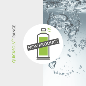
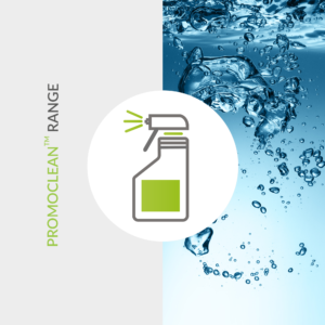
QUICKSOLV FIDES
- Oil & dust removal for dielectric cleaning
- For manual spray equipment
- Safe & fast cleaning under power
![]()
TOPKLEAN EL 10F
Misprint & Stencil Cleaning
Misprint and stencil cleaning in electronics helps maintain the accuracy and reliability of printed circuit boards by removing contaminants that could affect the quality of soldering and overall performance, with INVENTEC providing advanced solutions to ensure optimal results.
Effective stencil cleaning is crucial in SMT printing and PCB assembly to prevent misprints, with advanced solutions like TOPKLEAN EL 7 enhancing production quality in electronics and semiconductor manufacturing…
Learn more
Related products & services

Discover our high-perfoming solder stencils cleaner!
TOPKLEAN EL 606
- Stencil cleaning
- Aqeous spray or immersion process
- Fast cleaning with very low HSE impact
This is a product
Electronic & Semiconductor
Industrial Cleaning Solutions
Frequently Asked Questions (FAQ)
What are the main contaminants targeted in electronic assembly and semiconductor cleaning?
Typical contaminants include flux residues, ionic contamination, oils, photoresist residues, and sub-micron particles. These must be removed to prevent issues such as dendritic growth, corrosion, leakage currents, and reduced device reliability.
What is the difference between water-based and solvent-based cleaning solutions?
Water-based cleaners rely on detergents, surfactants, and saponifiers to dissolve fluxes and particles, making them environmentally friendly but requiring rinsing and drying. Solvent-based systems use engineered solvents with high solvency power, offering fast drying and precision cleaning where water is unsuitable.
How does ultrasonic or megasonic cleaning improve performance in semiconductor processing?
These methods use acoustic cavitation to dislodge particles. Ultrasonic (20–40 kHz) is effective for general cleaning, while megasonic cleaning (0.8–2 MHz) is essential for delicate wafers and advanced packaging, as it minimizes cavitation damage while ensuring fine particle removal.
Why is ultrapure water (UPW) critical in wafer cleaning?
UPW ensures that no additional contaminants are introduced during rinsing. Semiconductor-grade UPW must meet resistivity > 18 MΩ·cm, TOC < 10 µg/L, and extremely low particle levels, as even a single ionic impurity can impact device yield.
What role does the RCA clean play in semiconductor manufacturing?
The RCA sequence involves SC-1 (NH₄OH + H₂O₂ + H₂O) to remove organics and particles, followed by SC-2 (HCl + H₂O₂ + H₂O) to remove metallic ions. This standardized procedure remains a cornerstone of pre-oxidation wafer cleaning.
How do cleaning solutions impact long-term electronic reliability?
Residual contaminants can lead to electrochemical migration, corrosion, or electrical shorts. Proper industrial cleaning solutions ensure stable solder joints, conformal coating adhesion, and extended device lifetime, especially in high-reliability fields like aerospace and medical electronics.
How does INVENTEC support integration of cleaning solutions into existing production lines?
INVENTEC provides water- and solvent-based cleaning formulations optimized for spray-in-air, immersion, and ultrasonic equipment. Their expertise helps customers adapt cleaning chemistry to inline or batch systems without compromising throughput or reliability.
What emerging technologies are being explored in precision cleaning?
Alternatives include supercritical CO₂ cleaning, plasma cleaning, and Marangoni drying with IPA vapor. These methods reduce water usage, minimize residues, and provide highly controlled surface preparation for advanced semiconductor packaging.
What measures reduce the environmental impact of industrial cleaning?
Eco-focused strategies include closed-loop solvent recycling, lower temperature cleaning, microemulsion technology, and replacing high-VOC solvents with sustainable water-based alternatives. INVENTEC has developed formulations that combine process efficiency with reduced ecological footprint.
How does INVENTEC ensure process reliability after cleaning solution implementation?
INVENTEC supports its customers through lab testing, residue analysis, and on-site process optimization. This ensures that cleaning performance meets IPC and industry standards, while safeguarding long-term reliability of assemblies and wafers.
Electronic & Semiconductor Cleaning: Essential Guide for High-Performance Devices
Electronic and semiconductor cleaning solutions are critical for ensuring the performance, reliability, and longevity of high-precision electronic devices. Proper cleaning removes residues, contaminants, and particles from PCBs, semiconductor wafers, and sensitive assemblies.
Integrating industrial cleaning processes in production and rework lines reduces defect rates, improves thermal and electrical performance, and ensures compliance with industry standards for high-reliability electronics. These cleaning solutions are widely applied in automotive electronics, aerospace systems, and medical devices.
Benefits & Applications
Key BenefitsElectronic cleaning and semiconductor cleaning solutions ensure pristine PCBs, power electronics, and sensitive packages. These water-based and solvent-based cleaning solutions remove flux residues, contaminants, SMT glue, and misprints without damaging delicate components, improving component reliability and manufacturing yield.
Technical AspectsOur electronic cleaning and semiconductor cleaning solutions are formulated for diverse industrial processes, including PCB defluxing, power electronics cleaning, package cleaning, maintenance cleaning, and SMT glue cleaning. Optimized solvent selection and process parameters ensure efficient contaminant removal while maintaining substrate integrity.
ApplicationsThese electronic cleaning and semiconductor cleaning solutions are widely applied in automotive electronics, aerospace & defense modules, and medical electronic assemblies. Ideal for PCB defluxing, misprint & stencil cleaning, and maintenance of sensitive components, they enhance process reliability and help manufacturers comply with strict industry quality standards.
Electronic Cleaning Solutions in the Automotive Industry
In automotive electronics, including ECUs, sensor modules, and powertrain components, cleaning removes flux residues and particulates, ensuring consistent signal integrity and thermal management in high-reliability applications.
Electronic Cleaning Solutions in Aerospace & Defense
For aerospace electronics and defense systems, precise cleaning ensures avionics, radar modules, and satellite components are free from contaminants that could compromise signal quality and reliability in extreme conditions.
Electronic Cleaning Solutions in the Medical Industry
In medical devices, cleaning ensures PCBs, imaging sensors, and diagnostic electronics operate without contamination, guaranteeing accurate signal processing and patient safety.
Technical support
Inventec has a worldwide dedicated Technical Support team to help you along the different stages of our cooperation.
Depending on your request, we provide online or onsite support
- to select the right product based on your specific needs
- to assist you in your product qualification process
- to guide you with the initial set up of you process at all your worldwide manufacturing facilities
- to provide fast response on technical issues which could occur at any time during mass production.


Free-of-Charge cleaning trials
In order to know if our products reach your expectations on your specific part and according to your desired process, we provide FREE-OF-CHARGE cleaning trials in our Technical Centers. A comprehensive technical report detailing all test results and recommendations regarding process & process parameters will be provided. You want to attend the trials? We are happy to welcome you.