PoP Assembly Semiconductor Packaging Process
Our advanced soldering solutions for PoP assembly ensure precise interconnect formation, superior joint reliability, and optimal thermal and electrical conductivity—engineered to meet the exacting demands of high-density semiconductor packaging and stacked integrated circuit applications.
Maximizing Efficiency and Performance with Advanced PoP Assembly in Semiconductor Packaging
PoP assembly plays a vital role in modern semiconductor packaging, enabling space-efficient, high-performance integration of integrated circuits through advanced soldering solutions and precisely formulated solder paste.
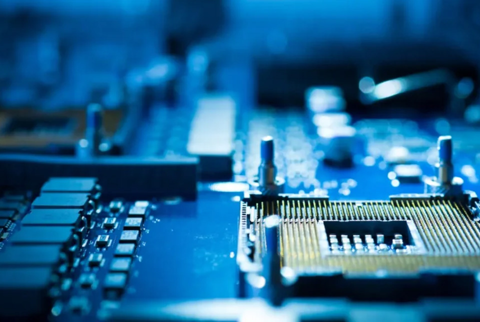
Package on Package (PoP) Assembly is a key innovation in semiconductor packaging that stacks multiple PoP components vertically, creating compact, multi-layered devices essential for smartphones, tablets, and wearables. This technique optimizes space without compromising speed or functionality.
Central to PoP assembly is the precise connection of stacked layers using specialized soldering solutions. Advanced solder pastes and fluxes engineered for rigorous semiconductor processes ensure reliable electrical and mechanical bonds, reducing defects like voiding or bridging and enhancing the durability and performance of PoP components.
Key Advantages of PoP Assembly Solutions:
- Vertical stacking of PoP components saves valuable board space
- Specialized solder pastes and fluxes minimize voids and improve joint reliability
- Optimized chemical formulations ensure thermal compatibility and excellent wetting
- Supports high-bandwidth connections between memory and logic chips
- Enables compact, high-performance devices for mobile and computing applications
INVENTEC’s expertly formulated solder pastes and fluxes for PoP assembly deliver high yields and reliable performance, empowering modern semiconductor packaging innovations.
See Other Semicon Packaging Processes Read FAQ
PRODUCT OVERVIEW
We only show below the most relevant and newest products in our range. If you don’t find a specific product, you will probably find it with our search option.
Showing all 2 results
-

ECOREL HT 301T
- Pb93,5Sn5Ag1,5 Leaded solder paste
- No clean printing process
- Low voids & high reliability

-


Discover our water-soluble tacky flux designed for flawless PoP and Flip Chip soldering!
ECOFREC POP WS30
- Water soluble tacky flux
- PoP and Flip Chip process
- Excellent wetting properties
PoP Assembly Semiconductor Packaging Process
Semiconductor Soldering Solutions
Frequently Asked Questions (FAQ)
What is Package on Package (PoP) assembly in semiconductor packaging?
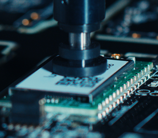
PoP assembly stacks multiple semiconductor packages vertically to increase functionality and save PCB space. Typically, a logic or processor package is mounted on top of a memory package, interconnected through solder balls or bumps.
How are the packages connected in PoP assembly?
Packages in PoP are connected using solder balls arranged on the top package’s substrate that mate with pads on the bottom package. These solder balls are reflowed to form reliable electrical and mechanical connections.
What types of solder pastes and fluxes are used in PoP assembly?
Low voiding solder pastes and tacky fluxes are commonly used to ensure strong, void-free joints in PoP assemblies. INVENTEC offers specialized flux and solder paste formulations that support high-reliability PoP processes.
What are the main advantages of PoP technology?
PoP enables increased component density, reduces PCB footprint, and improves electrical performance by shortening interconnect lengths. It supports heterogeneous integration, combining different chip technologies in one package.
What challenges are associated with PoP assembly?
Challenges include precise alignment of packages, controlling solder ball collapse, avoiding voiding, and managing thermal stresses. Flux selection and reflow profile optimization are critical to address these challenges effectively.
How is voiding minimized in PoP solder joints?
Using low voiding solder pastes combined with optimized reflow profiles and proper flux application helps minimize void formation. Vacuum reflow can also be employed for ultra-low voiding in PoP assemblies.
Is PoP assembly compatible with lead-free solder alloys?
Yes. Lead-free solder alloys like SAC305 are widely used in PoP to meet environmental regulations. INVENTEC provides lead-free solder pastes formulated to maintain excellent joint integrity in PoP processes.
What inspection methods verify PoP solder joint quality?
X-ray inspection is standard to detect voiding and solder joint defects. Other methods include shear testing and automated optical inspection (AOI) for package alignment and surface defects.
How does flux chemistry impact PoP assembly?
Flux chemistry influences wetting, oxidation removal, and residue cleanliness. High-performance fluxes like those from INVENTEC ensure strong joints with minimal residue and contamination in the stacked package environment.
Does INVENTEC supply materials specifically for PoP assembly?
Yes. INVENTEC Performance Chemicals offers a range of solder pastes and fluxes optimized for PoP assembly, designed to provide excellent wetting, low voiding, and high reliability in complex semiconductor packaging applications.
Technical support
Inventec has a worldwide dedicated Technical Support team to help you along the different stages of our cooperation.
Depending on your request, we provide online or onsite support
- to select the right product based on your specific needs
- to assist you in your product qualification process
- to guide you with the initial set up of you process at all your worldwide manufacturing facilities
- to provide fast response on technical issues which could occur at any time during mass production.


Free-of-Charge cleaning & coating trials
Do you need cleaning or coating after soldering? We provide FREE-OF-CHARGE cleaning or coating trials in our Technical Centers. A comprehensive technical report detailing all test results and recommendations regarding process & process parameters will be provided. It is also possible to attend trials in person.