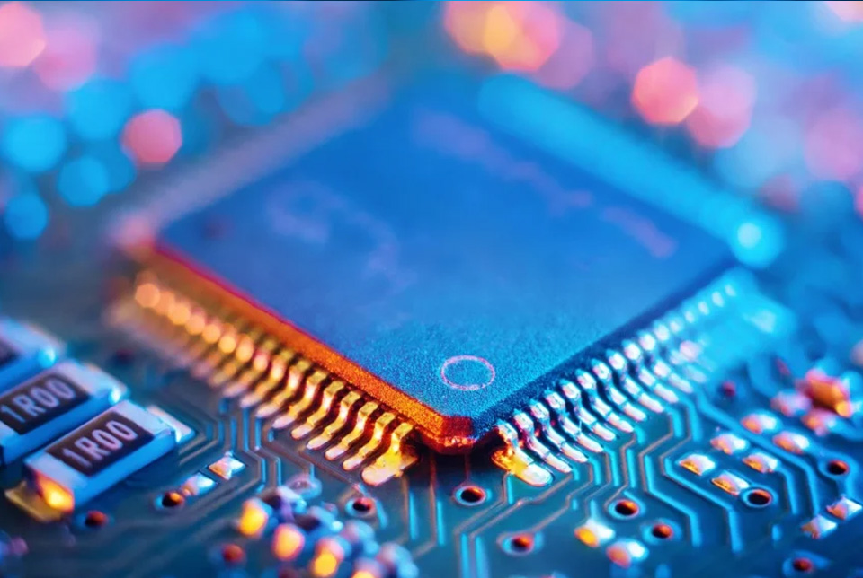
SiP Semiconductor Packaging Process
Our advanced soldering solutions for SiP semiconductor assembly guarantee precise interconnect formation, exceptional joint reliability, and enhanced thermal and electrical performance—engineered to meet the rigorous requirements of high-density system in package configurations and complex multi-chip semiconductor packaging.
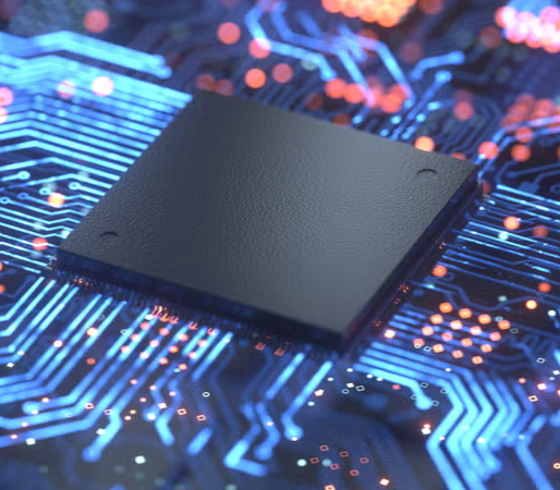
System-in-Package (SiP) Technology Transforming Semiconductor Packaging
System-in-Package (SiP) technology is transforming the semiconductor industry by integrating multiple integrated circuits into a single compact package, with advanced soldering solutions playing a crucial role in ensuring performance, reliability, and miniaturization.
System-in-Package (SiP) technology represents a groundbreaking advancement in the semiconductor packaging landscape. By integrating multiple integrated circuits (ICs) and passive components into a single compact module, SiP enables enhanced device performance, significant size reduction, and improved energy efficiency. This multi-chip packaging approach allows for higher functionality in smaller footprints, addressing the growing demand for miniaturization in consumer electronics, IoT devices, and wearable technology.
At the heart of successful SiP assembly lie the critical soldering solutions that ensure seamless electrical and mechanical interconnections between the various components. INVENTEC, a leader in semiconductor processes, offers advanced SiP solder paste and specialized chemical products designed specifically for the challenges of system in package manufacturing. Their portfolio includes high-performance solder paste, reliable solder bumps, fluxes, and underfills that play a vital role in the semiconductor packaging process.
Key Features of SiP Packaging Solutions:
- Integration of multiple ICs and passive components in compact modules
- Advanced solder paste and flux formulations for precise, durable bonding
- Robust thermal and mechanical stability under extreme conditions
- High adhesion and minimal defects ensuring long-term reliability
- Enables high-density, complex system configurations with improved energy efficiency
INVENTEC’s advanced SiP soldering solutions support manufacturers in achieving high yields, reliability, and performance in next-generation semiconductor packaging.
See Other Semicon Packaging Processes Read FAQ
PRODUCT OVERVIEW
We only show below the most relevant and newest products in our range. If you don’t find a specific product, you will probably find it with our search option.
Showing all 2 results
-

-
ECOREL FREE 300-31A
- N96,5AG3,5 lead free solder paste
- No clean SMT printing process
- Excellent low voiding for DCB


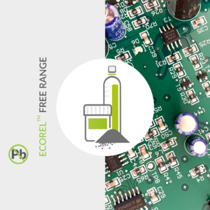

Discover our lead-free solder paste for high-reliability DCB assemblies with excellent low voiding results!

ECOREL FREE 300-31A
- N96,5AG3,5 lead free solder paste
- No clean SMT printing process
- Excellent low voiding for DCB
SiP (System-in-Package) Semiconductor Packaging Process
Semiconductor Soldering Solutions
Frequently Asked Questions (FAQ)
What is System-in-Package (SiP) technology in semiconductor packaging?
SiP technology integrates multiple semiconductor dies and passive components into a single compact package, enabling complex system functionality in a reduced footprint. SiP improves performance by combining heterogeneous components closely together.
How does SiP differ from traditional packaging methods?
Unlike single-die packages, SiP integrates multiple chips (logic, memory, sensors) within one package, often stacked or side-by-side, reducing interconnect lengths and improving electrical and thermal performance.
What soldering processes are used in SiP assembly?
SiP assembly uses advanced soldering methods including flip chip bonding, wire bonding, and die attach with specialized solder pastes and fluxes. INVENTEC provides materials optimized for these processes to ensure strong, reliable interconnects.
What challenges are associated with SiP packaging?
Challenges include managing thermal dissipation, precise die placement, void reduction, and ensuring mechanical integrity. Selecting high-performance solder pastes and fluxes with low voiding characteristics is crucial, as offered by INVENTEC.
What materials are used for die attach and interconnect in SiP?
Solder pastes, conductive adhesives, and underfill materials are commonly used. Solder alloys must provide excellent thermal and electrical conductivity, while flux chemistries support clean, void-free joints.
How is thermal management addressed in SiP?
SiP designs incorporate thermal vias, heat spreaders, and thermally conductive die attach materials to dissipate heat efficiently. High-performance solder pastes from INVENTEC contribute to effective thermal conduction within the package.
Is SiP assembly compatible with lead-free solder?
Yes. Lead-free solder alloys such as SAC305 are widely used in SiP to comply with environmental standards while maintaining high reliability. INVENTEC offers lead-free solder pastes optimized for SiP applications.
What inspection methods ensure SiP assembly quality?
X-ray and scanning acoustic microscopy (SAM) are used to detect voids, delamination, and solder joint defects. Optical inspection verifies die alignment and package integrity.
How does flux chemistry impact SiP assembly reliability?
Flux chemistry affects solder wetting, oxide removal, and residue cleanliness. Advanced fluxes like those from INVENTEC ensure strong solder joints with minimal residue, critical for high-density SiP packaging.
Does INVENTEC offer soldering materials for SiP technology?
Yes. INVENTEC Performance Chemicals provides a range of solder pastes and fluxes specifically engineered to meet the complex demands of SiP semiconductor packaging, focusing on low voiding, strong adhesion, and high thermal performance.
Technical support
Inventec has a worldwide dedicated Technical Support team to help you along the different stages of our cooperation.
Depending on your request, we provide online or onsite support
- to select the right product based on your specific needs
- to assist you in your product qualification process
- to guide you with the initial set up of you process at all your worldwide manufacturing facilities
- to provide fast response on technical issues which could occur at any time during mass production.


Free-of-Charge cleaning & coating trials
Do you need cleaning or coating after soldering? We provide FREE-OF-CHARGE cleaning or coating trials in our Technical Centers. A comprehensive technical report detailing all test results and recommendations regarding process & process parameters will be provided. It is also possible to attend trials in person.