Package Assembly Semiconductor Process
Our advanced sintering solutions for package assembly ensure robust electrical connections, enhanced joint durability, and superior thermal management—designed to meet the rigorous requirements of modern semiconductor packaging and high-performance device applications.
Advancing Semiconductor Packaging with the Critical Role of Package Assembly and Cutting-Edge Sintering Solutions
In the rapidly evolving world of semiconductor processes, the package assembly stage plays a crucial role in ensuring device performance and reliability, with innovative sintering solutions emerging as a game-changing technology for advanced semiconductor packaging.
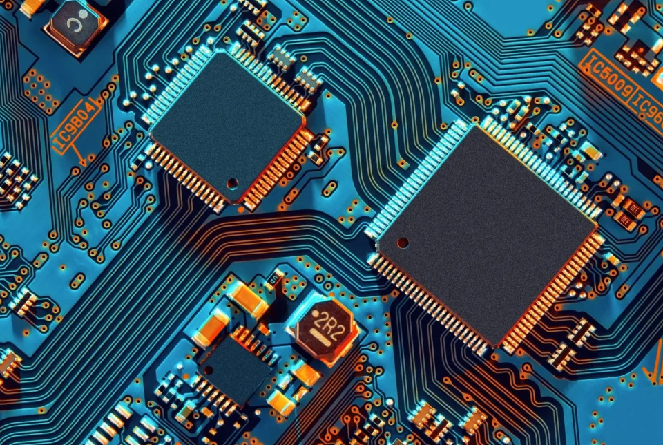
The package assembly process is a pivotal stage within semiconductor processes, where the bare silicon die is electrically and mechanically connected to the external leads of the package. This crucial step enables the semiconductor device to interface seamlessly with the broader electronic system. Traditionally, methods such as wire bonding and flip-chip have been employed to establish these vital electrical connections. However, recent advancements in semiconductor packaging have brought sintering solutions to the forefront as a superior bonding technology.
Integrating advanced sintering solutions into the package assembly process delivers significant performance improvements, particularly in high-reliability and high-power applications. The use of sintering paste — a specialized conductive material — facilitates the formation of strong, low-resistance joints between the die and the package substrate. This results in enhanced electrical conductivity, superior thermal dissipation, and improved mechanical robustness, all of which are critical for sustaining the longevity and efficiency of modern semiconductor devices.
Highlights of Package Assembly with Sintering Solutions:
- Strong, low-resistance joints formed by specialized sintering paste
- Enhanced electrical conductivity and superior thermal dissipation
- Improved mechanical robustness supporting device longevity
- Enabling advanced configurations like SiP and 3D stacked die designs
- Supports miniaturization, multifunctionality, and high power efficiency
Explore INVENTEC’s advanced sintering solutions to elevate your package assembly and semiconductor manufacturing capabilities.
See Other Semicon Packaging Processes Read FAQ
PRODUCT OVERVIEW
We only show below the most relevant and newest products in our range. If you don’t find a specific product, you will probably find it with our search option.
Showing all 6 results
-

-
-
-

Tailor-made solution
You do not find the perfect product ? We can also offer you some tailor-made solutionContact Us -
-
-
Discover our advanced low-pressure silver sintering paste for reliable high-power assembly!

ECOREL SINTEC AP90
- AG Sintering Paste
- Low Pressure Sintering
- Printing
Package Assembly Semiconductor Process
Semiconductor Soldering Solutions
Frequently Asked Questions (FAQ)
What is the semiconductor package assembly process?
The semiconductor package assembly process involves encapsulating the semiconductor die in a protective package that facilitates electrical connections to the outside world. This includes die attach, wire bonding or flip chip attachment, molding, soldering, and final testing.
What are the main steps involved in semiconductor package assembly?
Key steps include die attach to the substrate, wire bonding or flip chip bumping for interconnects, molding or encapsulation, soldering the package to PCB or substrates, and rigorous inspection and testing to ensure reliability.
What types of soldering processes are used in package assembly?
Common soldering processes include reflow soldering for surface mount, wave soldering for through-hole, and selective soldering for complex assemblies. INVENTEC supplies solder pastes and fluxes designed for optimal performance in these processes.
How important is flux in semiconductor package assembly?
Flux is critical for removing oxides and promoting good wetting during soldering. High-quality flux formulations, such as those offered by INVENTEC, ensure strong, reliable solder joints and minimal residues for improved assembly yield.
What solder alloys are typically used in semiconductor package assembly?
Lead-free alloys like SAC305 (SnAgCu) dominate due to environmental regulations. Some applications still use SnPb alloys. INVENTEC provides compatible solder pastes formulated for both lead-free and traditional alloys.
What challenges are common in semiconductor package assembly?
Challenges include void formation, solder joint reliability, thermal management, and precise component placement. Controlling solder paste printing, flux application, and reflow profiles is essential for high-quality assembly.
How is voiding controlled in package assembly solder joints?
Using low voiding solder pastes, optimized flux chemistries, controlled reflow profiles, and sometimes vacuum reflow ovens helps minimize voids, enhancing thermal and electrical performance of the package.
What inspection techniques are used to ensure package assembly quality?
X-ray inspection is widely used to detect internal voids and solder joint defects. Other methods include Automated Optical Inspection (AOI) and mechanical testing for reliability assurance.
Does INVENTEC offer materials for semiconductor package assembly?
Yes, INVENTEC Performance Chemicals offers a broad portfolio of solder pastes, fluxes, and other assembly materials tailored for semiconductor package assembly, supporting high yield, reliability, and advanced packaging technologies.
How does package assembly impact overall semiconductor device performance?
Reliable package assembly ensures mechanical protection, electrical connectivity, and thermal management of the semiconductor device, directly influencing device longevity, performance, and customer satisfaction.
Technical support
Inventec has a worldwide dedicated Technical Support team to help you along the different stages of our cooperation.
Depending on your request, we provide online or onsite support
- to select the right product based on your specific needs
- to assist you in your product qualification process
- to guide you with the initial set up of you process at all your worldwide manufacturing facilities
- to provide fast response on technical issues which could occur at any time during mass production.


Free-of-Charge cleaning & coating trials
Do you need cleaning or coating after soldering? We provide FREE-OF-CHARGE cleaning or coating trials in our Technical Centers. A comprehensive technical report detailing all test results and recommendations regarding process & process parameters will be provided. It is also possible to attend trials in person.