Flip Chip & CSP Semiconductor Packaging Process
Our advanced Flip Chip and CSP solutions are designed to deliver precise, reliable flip chip bonding with superior solder bump integrity, excellent thermal and electrical performance, and robust mechanical strength—perfectly suited for high-volume semiconductor packaging and demanding flip chip process applications.
Elevating Semiconductor Packaging Through Flip Chip and CSP Solutions
In today’s cutting-edge semiconductor industry, flip chip and CSP technologies are transforming packaging processes by enabling higher performance, greater miniaturization, and improved reliability through innovative flip chip bonding and advanced semiconductor soldering solutions.
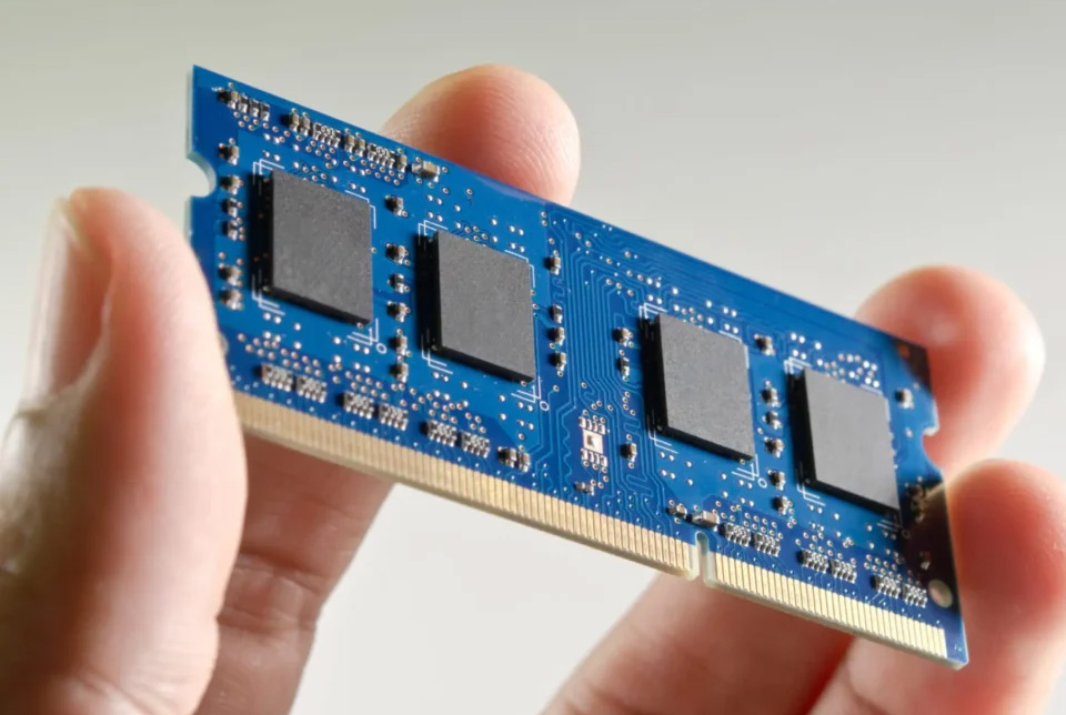
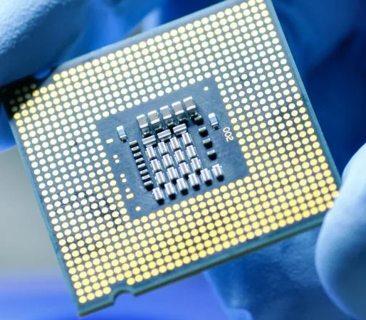
In the rapidly evolving world of semiconductor packaging, flip chip and Chip-on-Substrate Packaging (CSP) technologies have fundamentally transformed how electronic components are assembled and integrated. These advanced packaging methods enable unprecedented miniaturization, improved electrical performance, and superior thermal management, addressing the growing demands of modern high-performance semiconductor devices.
At the heart of this revolution lies the flip chip process, where the semiconductor die is flipped upside down and connected directly to the chip substrate or the underlying substrate via an array of microscopic solder bumps. This direct connection eliminates the need for traditional wire bonding, resulting in shorter signal paths and enhanced device speed. Flip chip bonding also improves electrical conductivity and heat dissipation, ideal for applications in computing, telecommunications, and consumer electronics.
Key Benefits of Flip Chip and CSP Solutions:
- Direct die-to-substrate connection improving signal speed and integrity
- Enhanced thermal management for high-performance devices
- Support for multi-chip stacking via chip on wafer on substrate (CoWoS) techniques
- High-density interconnections with superior mechanical reliability
- Compatibility with advanced semiconductor packaging formats
INVENTEC’s semiconductor soldering solutions optimize the flip chip assembly process by ensuring consistent solder bump formation and robust bonding quality, empowering manufacturers to achieve superior device performance and longevity.
See Other Semicon Packaging Processes Read FAQ
PRODUCT OVERVIEW
We only show below the most relevant and newest products in our range. If you don’t find a specific product, you will probably find it with our search option.
Showing all 2 results
-

-
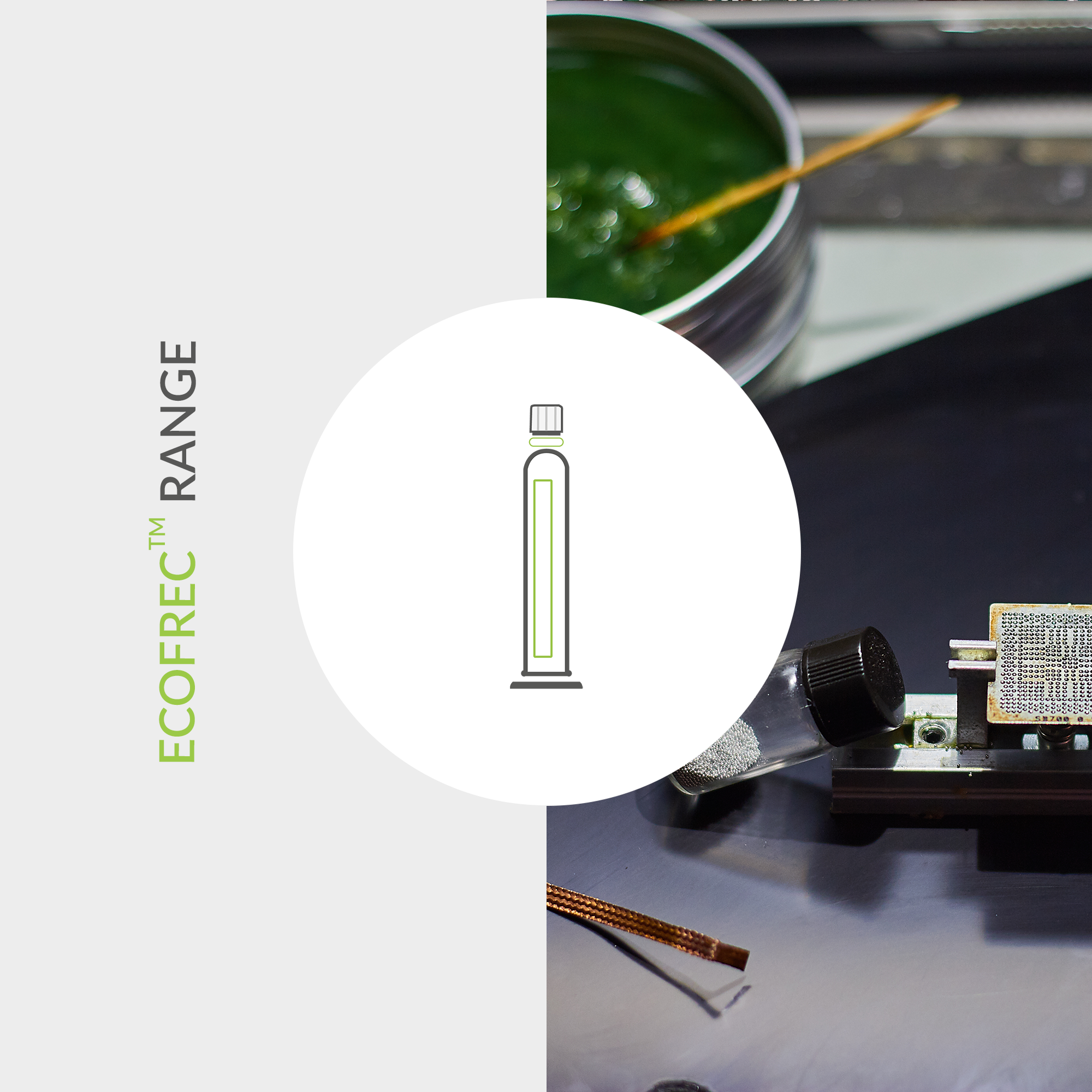
ECOFREC TF48
- No clean tacky flux
- Flip Chip, spheres soldering & components rework
- Excellent printing & high viscosity


Discover our water-soluble tacky flux designed for flawless PoP and Flip Chip soldering!
ECOFREC POP WS30
- Water soluble tacky flux
- PoP and Flip Chip process
- Excellent wetting properties
Flip Chip & CSP Semiconductor Packaging Process
Semiconductor Soldering Solutions
Frequently Asked Questions (FAQ)
What is flip chip packaging in semiconductor assembly?
Flip chip packaging involves mounting a semiconductor die upside down (face down) onto a substrate or PCB, using solder bumps as the electrical and mechanical interconnects. This approach enables shorter interconnects and better electrical performance than traditional wire bonding.
What does CSP stand for and how is it related to flip chip?
CSP stands for Chip Scale Package, a miniaturized packaging technology often utilizing flip chip techniques. CSPs provide a compact footprint nearly the same size as the die itself, improving performance and enabling miniaturization in electronics.
What are solder bumps in flip chip packaging?
Solder bumps are tiny spheres of solder placed on the die pads that form the connection between the die and substrate during reflow. These bumps act as the physical and electrical bridges and are critical to the flip chip process.
How is flux used in flip chip and CSP packaging?
Flux is applied to promote wetting and oxide removal during solder bump reflow. Specialized tacky or liquid fluxes are used to hold solder bumps in place and ensure robust solder joint formation. INVENTEC supplies advanced flux formulations optimized for flip chip and CSP.
What solder alloys are commonly used for flip chip and CSP?
Lead-free alloys such as SAC305 (SnAgCu) are common for flip chip and CSP due to RoHS compliance. Some applications may still use SnPb alloys depending on reliability needs. INVENTEC offers solder pastes compatible with both lead-free and traditional alloys.
What are typical challenges in flip chip and CSP processes?
Challenges include solder bump misalignment, voiding, insufficient wetting, and stress-induced joint failure. Controlling flux chemistry, solder paste printing, and reflow profiles is critical for high-yield packaging. INVENTEC supports these needs with tailored materials.
How does flip chip packaging benefit electronic device performance?
Flip chip reduces parasitic inductance and resistance by shortening interconnects, improving signal speed and power distribution. CSP reduces package size, supporting miniaturization and enhanced thermal management.
What inspection methods are used for flip chip and CSP solder joints?
X-ray inspection is the primary method to detect voiding and solder joint integrity. Automated optical inspection (AOI) and scanning acoustic microscopy (SAM) are also employed to ensure package reliability.
Are flip chip and CSP packaging processes compatible with vacuum reflow?
Yes. Vacuum reflow can significantly reduce voiding and improve solder joint reliability in flip chip and CSP packaging. INVENTEC fluxes and solder pastes are optimized for such advanced reflow environments.
Does INVENTEC provide solutions for flip chip and CSP packaging?
INVENTEC Performance Chemicals offers specialized solder pastes and fluxes designed for flip chip and CSP semiconductor packaging. Their products focus on low voiding, excellent wetting, and high reliability required in these advanced packaging technologies.
Technical support
Inventec has a worldwide dedicated Technical Support team to help you along the different stages of our cooperation.
Depending on your request, we provide online or onsite support
- to select the right product based on your specific needs
- to assist you in your product qualification process
- to guide you with the initial set up of you process at all your worldwide manufacturing facilities
- to provide fast response on technical issues which could occur at any time during mass production.


Free-of-Charge cleaning & coating trials
Do you need cleaning or coating after soldering? We provide FREE-OF-CHARGE cleaning or coating trials in our Technical Centers. A comprehensive technical report detailing all test results and recommendations regarding process & process parameters will be provided. It is also possible to attend trials in person.