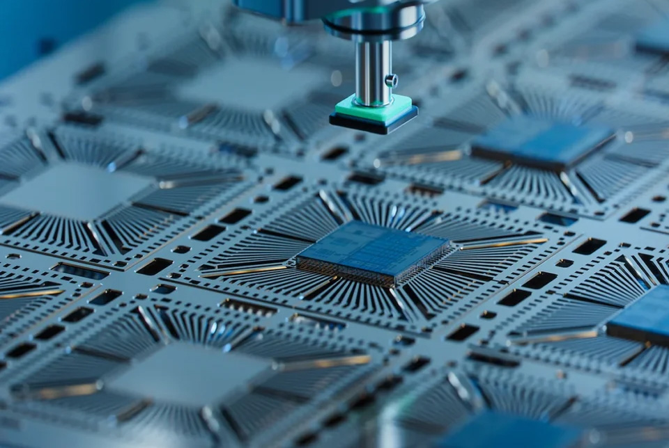
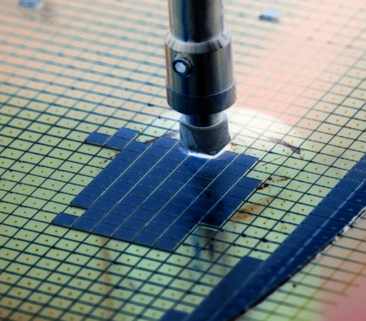
Die Attach Semiconductor Packaging Process
Our advanced die attach solutions ensure precise application, strong adhesion, and excellent thermal and electrical performance—ideal for high-volume semiconductor packaging and demanding die bonding applications.
Innovative Die Attach Solutions Driving Modern Semiconductor Packaging
As semiconductor devices grow more powerful and compact, advanced die attach technologies are essential to maintain performance, reliability, and thermal management in semiconductor packaging. The die attach process bonds the semiconductor die to substrates, ensuring strong adhesion, excellent conductivity, and effective heat dissipation.
A wide range of die attach materials including die attach solder paste, sintering paste, die attach adhesive, and lead-free solder paste are tailored to diverse applications. Notably, sintering die attach stands out for superior thermal and electrical conductivity, particularly in power electronics and automotive sectors.
Effective die bonding addresses challenges like CTE mismatch, moisture resistance, and void minimization. Innovations in die attach formulations improve thermal cycling stability and compatibility across substrates and metallizations, enhancing device longevity and performance.
Key Features of Modern Die Attach Solutions:
- Wide variety of die attach materials for specialized applications
- Superior thermal and electrical conductivity with sintering paste
- Epoxy-based die attach adhesives offering strong adhesion and easy handling
- Innovations to reduce voids and improve thermal cycling stability
- Eco-friendly and low-temperature sintering trends for sustainable electronics
INVENTEC’s die attach technologies combine durability and thermal management to meet the evolving demands of semiconductor packaging.
See Other Semicon Packaging Processes Read FAQ
PRODUCT OVERVIEW
We only show below the most relevant and newest products in our range. If you don’t find a specific product, you will probably find it with our search option.
Showing all 2 results
-

ECOREL HT 301T
- Pb93,5Sn5Ag1,5 Leaded solder paste
- No clean printing process
- Low voids & high reliability

-
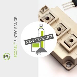
Discover Our Pressureless Sintering Paste for High-Power Die Attach and SiC/GaN Applications!

ECOREL SINTEC XP95D
- AG Sintering Paste
- Pressureless Sintering
- Dispensing
Die Attach Semiconductor Packaging Process
Semiconductor Soldering Solutions
Frequently Asked Questions (FAQ)
What is the die attach process in semiconductor packaging?
Die attach is the process of bonding a semiconductor die to a substrate, lead frame, or package using an adhesive or solder material. It is a critical step in forming mechanical support and ensuring thermal and electrical performance in semiconductor devices.
What materials are used for die attach?
Die attach can use conductive adhesives, solder pastes, or sintering materials. For high-power or high-reliability applications, solder-based die attach (using Ag-based or AuSn alloys) is preferred. INVENTEC offers advanced solder pastes tailored for die attach in demanding applications.
What is solder-based die attach?
Solder-based die attach involves applying a solder paste or preform between the die and substrate, then reflowing to form a metallic bond. This method provides excellent thermal conductivity and long-term mechanical reliability, ideal for power electronics and automotive semiconductors.
Why is thermal conductivity important in die attach?
Efficient thermal transfer from the die to the substrate is essential to prevent overheating and ensure device longevity. High-conductivity die attach materials, such as those offered by INVENTEC, help dissipate heat effectively in power and RF applications.
What role does flux play in solder-based die attach?
Flux removes surface oxides, promotes wetting, and ensures strong intermetallic bonding during the reflow process. INVENTEC formulates ultra-clean die attach fluxes with minimal residue, which are critical for fine-pitch dies and sensitive semiconductor packages.
What are the key challenges in die attach processes?
Key challenges include die misalignment, voiding, poor wetting, and solder bleed. Precise material selection and reflow control are vital to overcome these. INVENTEC provides solder solutions designed to minimize voids and ensure strong, reliable die bonds.
Is die attach compatible with lead-free solder?
Yes. Lead-free solder pastes, such as SnAgCu or other high-melting-point alloys, are widely used in modern die attach processes to meet RoHS and environmental regulations. INVENTEC offers RoHS-compliant options with optimized thermal and mechanical properties.
Can die attach solder paste be printed or dispensed?
Die attach solder paste is available for stencil printing, dispensing, or pin transfer methods. Selection depends on die size, placement precision, and production scale. INVENTEC offers formulations suitable for automated and manual application systems.
What inspection methods are used after die attach?
X-ray inspection is commonly used to detect voids and confirm die alignment. Optical inspection and shear testing may also be used to ensure bonding quality. Reliable material performance from INVENTEC simplifies process control and inspection validation.
Does INVENTEC offer die attach solder solutions?
Yes. INVENTEC Performance Chemicals supplies high-purity solder pastes and fluxes engineered specifically for die attach in semiconductor packaging. These materials offer low voiding, strong adhesion, and excellent thermal performance across multiple device types.
Technical support
Inventec has a worldwide dedicated Technical Support team to help you along the different stages of our cooperation.
Depending on your request, we provide online or onsite support
- to select the right product based on your specific needs
- to assist you in your product qualification process
- to guide you with the initial set up of you process at all your worldwide manufacturing facilities
- to provide fast response on technical issues which could occur at any time during mass production.


Free-of-Charge cleaning & coating trials
Do you need cleaning or coating after soldering? We provide FREE-OF-CHARGE cleaning or coating trials in our Technical Centers. A comprehensive technical report detailing all test results and recommendations regarding process & process parameters will be provided. It is also possible to attend trials in person.