Ball Attach Semiconductor Packaging Process
Our advanced ball attach solutions are engineered to provide precise, reliable solder ball attach performance with excellent wetting, strong mechanical bonds, and consistent electrical connectivity—ideal for high-volume semiconductor packaging and demanding BGA ball attach process applications.
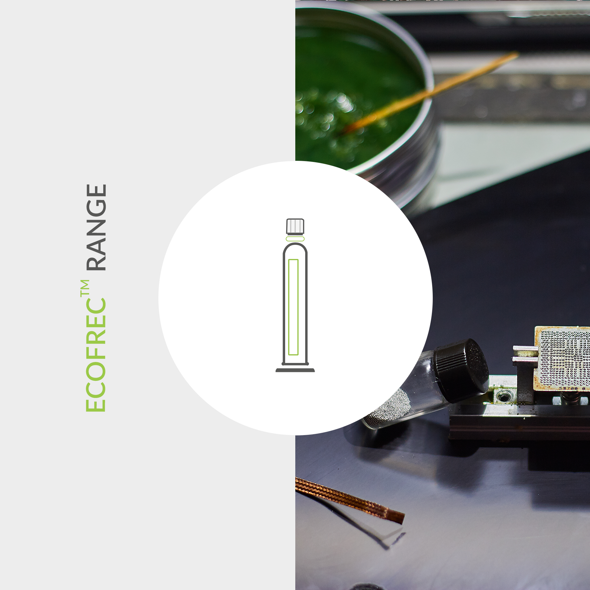
Advanced Solutions for the Ball Attach Semiconductor Packaging Process
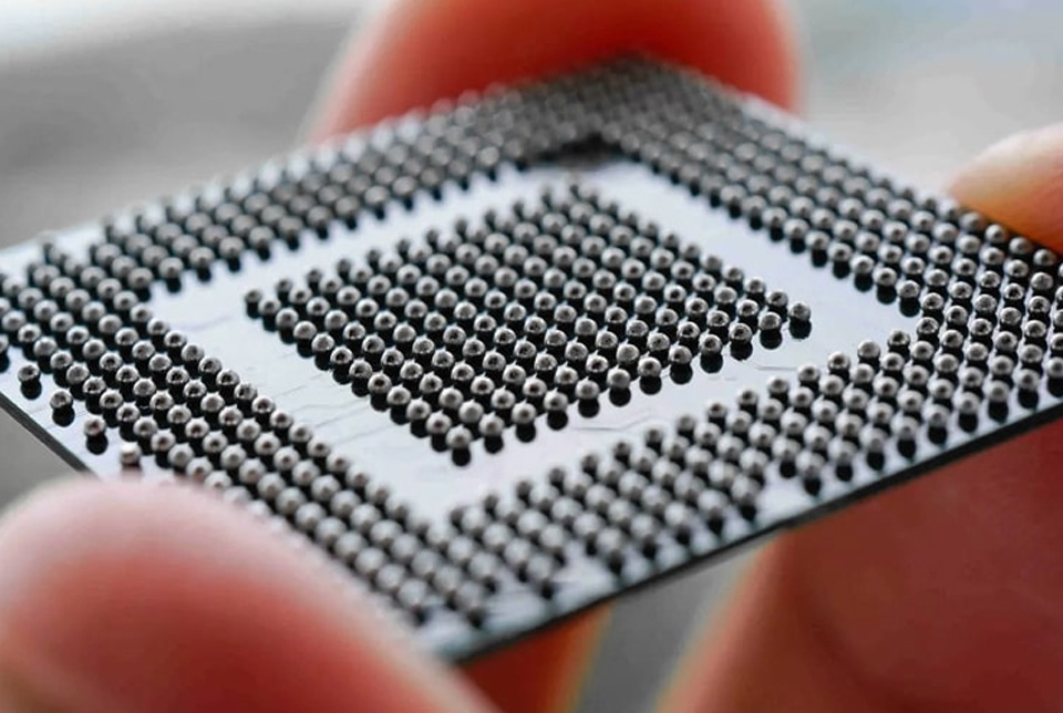
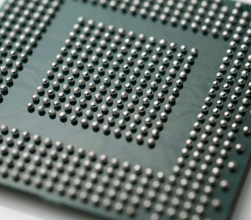
Modern semiconductor packaging depends on precise ball attach techniques to create reliable electrical and mechanical connections in Ball Grid Array (BGA) packages. The quality of the solder ball attach process directly impacts device performance and durability.
The BGA ball attach process involves placing and reflowing solder balls—or solder spheres—onto substrates or wafers, forming critical contact points between the silicon die and PCB. To meet high standards, specialized fluxes, solder pastes, and alloys ensure excellent wetting, strong adhesion, and minimized voiding for robust joints.
These advanced materials support both initial solder ball attach and BGA reballing for repair or rework. Compatible with lead-free and leaded solder spheres, they adapt to various substrates and package formats—from wafer-level to board-level semiconductor packaging processes.
Key Benefits of Advanced Ball Attach Solutions:
- Optimized solder ball attach formulations for consistent, high-yield production
- Broad compatibility with lead-free and leaded solder spheres
- Tailored fluxes and pastes for both BGA ball attach process and BGA reballing
- Minimized voiding and improved joint reliability through superior wetting
- Applicable across wafer-level, chip-scale, and other semiconductor packaging levels
INVENTEC’s solutions enhance ball attach reliability with tailored fluxes and alloys designed for high-yield semiconductor packaging processes.
See Other Semicon Packaging Processes Read FAQ
PRODUCT OVERVIEW
We only show below the most relevant and newest products in our range. If you don’t find a specific product, you will probably find it with our search option.
Showing all 2 results
-

-
ECOFREC TF48
- No clean tacky flux
- Flip Chip, spheres soldering & components rework
- Excellent printing & high viscosity

Discover Our Halogen-Free No-Clean Tacky Flux for All Your Soldering Needs!
ECOFREC TF49
- Halogen free tacky flux
- Flip Chip & Rework soldering
- Low residue properties
Ball Attach Semiconductor Packaging Process
Semiconductor Soldering Solutions
Frequently Asked Questions (FAQ)
What is the ball attach process in semiconductor packaging?
The ball attach process involves placing solder balls onto the pads of a semiconductor package (typically BGA or CSP) to create electrical and mechanical connections between the chip and the PCB. These solder balls are reflowed to form solid joints.
Why is ball attach important in semiconductor assembly?
Ball attach ensures reliable electrical connectivity and mechanical stability in fine-pitch semiconductor packages. It’s essential for flip-chip packaging, BGA rework, and wafer-level packaging. Consistent ball quality and flux selection are critical for yield.
What types of flux are used in ball attach processes?
Tacky flux and liquid flux are both used in ball attach. Tacky flux helps hold the solder balls in place prior to reflow, while liquid flux can be used for dipping or spraying. INVENTEC provides specialized fluxes designed for high-reliability ball attach applications.
What is the difference between wafer-level and package-level ball attach?
Wafer-level ball attach is performed on entire wafers before dicing, often using flux dipping or printing methods. Package-level ball attach is done after individual chip packaging, typically with tacky flux application. Both processes require precise flux control and solder ball placement.
What are the typical solder alloys used in ball attach?
Common solder alloys include lead-free compositions such as SAC305 and SnAgCu, as well as SnPb for legacy applications. INVENTEC supports a range of RoHS-compliant solder materials optimized for semiconductor packaging reliability and joint performance.
How are solder balls applied in the ball attach process?
Solder balls are typically applied by screen printing, ball placement machines, or ball transfer methods using tacky flux as an adhesive layer. Uniform ball height and alignment are essential to ensure successful reflow and joint formation.
What reflow conditions are used in ball attach?
Reflow profiles are carefully tuned to match the solder alloy and flux used. Profiles typically include a preheat, soak, and controlled peak temperature phase to ensure proper wetting, minimal voiding, and ball collapse. INVENTEC provides reflow guidance based on your materials.
Do ball attach fluxes require cleaning?
It depends on the flux type. No-clean fluxes may leave minimal residue suitable for high-reliability environments. Water-soluble or rosin-based fluxes typically require post-reflow cleaning to prevent corrosion or contamination. INVENTEC offers both no-clean and cleanable fluxes for ball attach.
What defects can occur in the ball attach process?
Common defects include ball misalignment, non-wet opens, head-in-pillow (HIP), voiding, and insufficient collapse. These can result from improper flux selection, solder ball contamination, or suboptimal reflow conditions. Proper process control is essential.
Does INVENTEC offer solutions for ball attach applications?
Yes. INVENTEC Performance Chemicals provides high-performance tacky and liquid fluxes tailored for semiconductor ball attach processes. These materials support both wafer-level and package-level operations with excellent wetting, low voiding, and minimal residue.
Technical support
Inventec has a worldwide dedicated Technical Support team to help you along the different stages of our cooperation.
Depending on your request, we provide online or onsite support
- to select the right product based on your specific needs
- to assist you in your product qualification process
- to guide you with the initial set up of you process at all your worldwide manufacturing facilities
- to provide fast response on technical issues which could occur at any time during mass production.


Free-of-Charge cleaning & coating trials
Do you need cleaning or coating after soldering? We provide FREE-OF-CHARGE cleaning or coating trials in our Technical Centers. A comprehensive technical report detailing all test results and recommendations regarding process & process parameters will be provided. It is also possible to attend trials in person.